Laser printer/xerox machine
Plain paper (A4)
Iron
Masking tape
Correction pen
Copper board.
Sand paper
Thinner
Procedure:
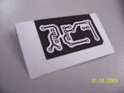
1. Print/photocopy the circuit of the design onto any plain paper.
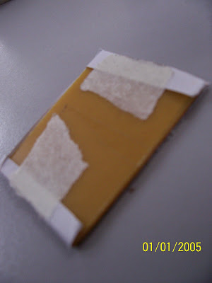
2. Cut copper board to the exact size of the artwork layout.
3. Use sand paper to remove copper oxidation and clean the surface oil residue. 4. Tape the printed artwork paper onto the board to avoid the paper from moving. Remember the artwork must be on the copper side.
 5. Making sure the paper facing up.
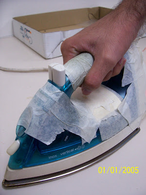
 6. Place the iron on top of the paper, apply some force on the iron (about 3~5 minutes)
7. Let the board cool down, and soak it with water until the paper soften (visible artwork).
 8. Gently scrub so that the paper comes out, and leaving behind the artwork.
 9. Examine the board for any correction. Using a correction pen to edit the printed PCB.
 10. After correction the board is ready for etching
 NOTE: This post wouldn't be complete without the help of my students act as my model.... hand model. hahah...
Thanks